





Development of Diamond Semiconductor Materials
-
摘要: 金刚石因其超宽禁带、高热导率、高击穿场强和优异的载流子迁移率,成为新一代半导体材料的典型代表,受到功率电子、射频通讯、量子信息等领域的广泛关注。本征单晶金刚石是发展金刚石半导体的基石,其杂质浓度需达10−9(parts per billion,ppb)级且位错密度极低。高温高压(high pressure high temperature,HPHT)法可获得更高的纯度与更好的晶体质量,但受限于尺寸,常作为化学气相沉积(chemical vapor deposition,CVD)外延的基底,以实现大尺寸高质量单晶制备。在掺杂方面,B原子因尺寸与C原子相近(差异仅6.5%),易于进入晶格形成性能优异的p型金刚石,相关器件(如肖特基二极管)已获成功。然而,n型掺杂面临根本挑战:P、S等潜在掺杂原子半径远大于C原子(差异35%~57%),难以掺入并激活。超高压高温热扩散法通过调控原子尺寸差异,有望成为实现浅能级n型掺杂的新途径。表面终端中,氢终端可诱导高迁移率二维空穴气,氧终端则提升界面稳定性,但两者的热稳定窗口(分别约为400、600 ℃)仍低于元素掺杂体系,限制了其在高温高频器件中的应用。因此,突破n型掺杂、提升终端热稳定性、发展大尺寸低成本制备工艺,将是推动金刚石半导体在功率电子、量子信息及高性能传感等领域迈向产业化的关键。本综述对上述问题进行了分析与讨论,并探讨了金刚石半导体的发展前景与困境。Abstract: Diamond has emerged as a quintessential representative of next-generation semiconductor materials, owing to its ultra-wide bandgap, exceptional thermal conductivity, high breakdown field strength, and outstanding carrier mobility. It has thus attracted extensive attention from fields such as power electronics, radio-frequency communications, and quantum information technologies. Intrinsic single-crystal diamond serves as the foundational substrate for diamond semiconductor development, requiring impurity concentrations at the parts per billion (ppb) level and extremely low dislocation densities. While the high-pressure high-temperature (HPHT) method yields material of higher purity and superior crystal quality, its utility is limited by small crystal dimensions. Consequently, HPHT-grown diamond is frequently employed as a substrate for chemical vapour deposition (CVD) homoepitaxy, enabling the preparation of large-area, high-quality single crystals. Regarding doping, the boron (B) atom, with a size difference of merely 6.5% compared to carbon (C), readily incorporates into the diamond lattice, facilitating the production of high-performance p-type diamond. Related devices, such as Schottky barrier diodes, have been successfully demonstrated. In contrast, n-type doping presents a fundamental challenge: potential dopants like phosphorus (P) and sulphur (S) possess atomic radii 35%–57% larger than carbon, making their incorporation and activation within the lattice exceedingly difficult. The ultra-high pressure and high-temperature diffusion method, which modulates this atomic size disparity under extreme pressures (e.g., about 15 GPa), emerges as a promising new pathway towards achieving shallow-level n-type doping. Concerning surface terminations, hydrogen termination induces a high-mobility two-dimensional hole gas (2DHG), whilst oxygen termination enhances interface stability and provides chemical passivation. However, their thermal stability windows (approximately 400 and 600 ℃, respectively) remain inferior to those of substitutionally doped diamond, limiting their application in high-temperature and high-frequency devices. Therefore, breakthroughs in n-type doping, enhanced thermal stability of surface terminations, and the development of large-area, cost-effective fabrication processes are critical to advancing diamond semiconductor technology towards commercialisation in power electronics, quantum technologies, and high-performance sensing. This review aims to analyse and discuss these pivotal issues, exploring both the prospects and the persistent challenges facing diamond semiconductor development.
-
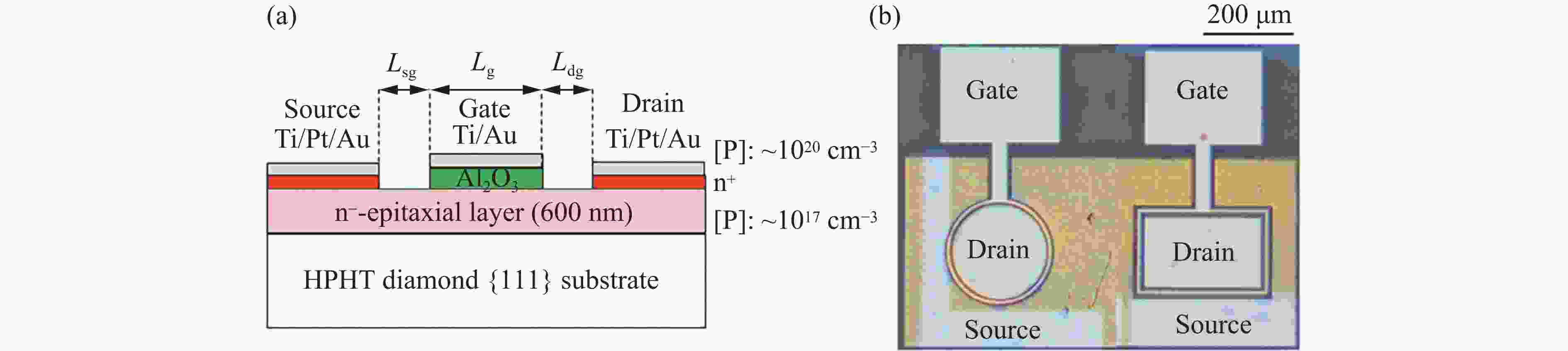
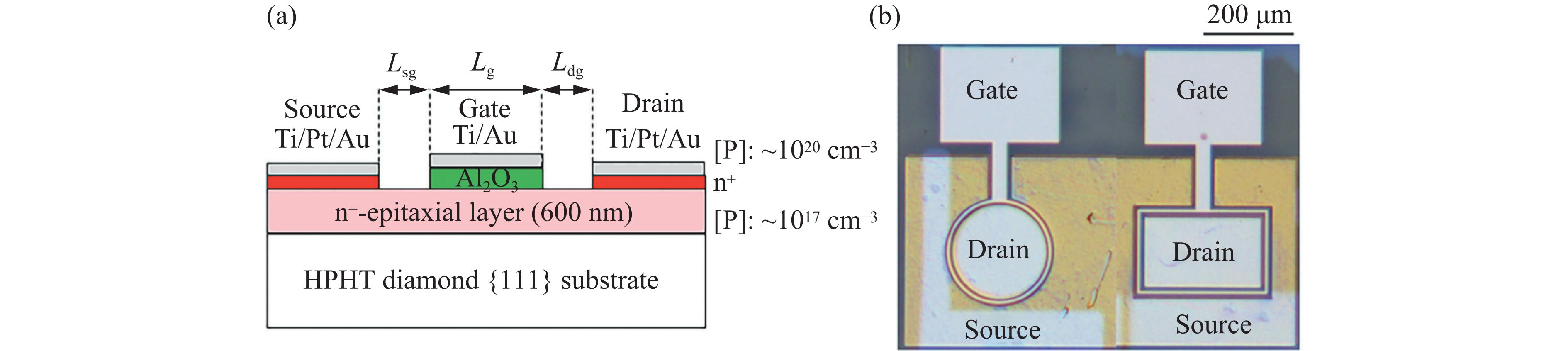
图 6 基于P掺杂n型金刚石的MOSFET:(a) MOSFET示意图(n+金刚石层用于降低源极和漏极的接触电阻,n−金刚石层用作沟道);(b) 金刚石MOSFET的光学图像[96]
Figure 6. MOSFETs based on phosphorous doped n-type diamond: (a) schematic of the MOSFETs (The n+ diamond layer is used to reduce the source and drain contact resistance, and the n− diamond layer serves as the channel.); (b) optical image of the diamond MOSFETs[96]
表 1 不同单晶金刚石衬底性能汇总
Table 1. Summary of properties of different single-crystal diamond substrates
Method Crystal quality/
typical sizePurity Defect density/
cm−2Typical application
scenariosRef. HPHT Single crystal, millimeter-to-centimeter scale, up to 15 carat N content 0.1–10−4,
Ⅱa <10−6103–105
(Ⅱa, optimized)High-power devices, quantum, cutting tools, CVD seeding [37–39] MPCVD Single crystal, millimeter-to-centimeter scale, up to
30 mm×30 mmImpurities<10−6,
N/B/Si well-controlled102–104
(high-quality epitaxy)High-end semiconductors, quantum, optics, epitaxy [40–41] HFCVD Single/polycrystal, millimeter-to-centimeter scale, thick films Impurities at 10−6 level, affected by filament 104–106 Large-area films, composite structures, thermal management, some electronics/optics [42] Explosion method Poly/nanocrystalline, micrometer-to-
millimeter scaleHigher impurities
(N, H, metals, etc.)106–108 Abrasives, polishing, thermal interface, large-volume industry [43]  下载: 导出CSV
表 2 P掺杂金刚石性能
Table 2. Properties of P-doped diamond
Doping concentration/
(ion·cm−3)Resistivity/
(Ω·cm)Mobility/
(cm2·V−1·s−1)Carrier concentration/
(ion·cm−3)Doping methods Ref. 2.3×10²⁰ 9.26 CVD [87] 1.2×10²⁰ 42 CVD [88] 1.2×10²⁰ 70 CVD [89] 3.56×10⁶ 313.27 5.59×10⁹ HPHT [90] 2×10¹⁸ 350 1×10¹¹ CVD [91] 4.8×10¹⁶ 1.8×10³ 1×10¹³ CVD [92] 2×10¹⁵ 1 060 1×10¹⁰ CVD [93] 7.07×10¹⁹ 0.83 2.78 2.72×10¹⁸ HPHT-TD [94]
下载: 导出CSV
-
[1] BOLSHAKOV A P, YUROV V Y, FEDOROVA I A, et al. Growth of homoepitaxial single crystal diamond by microwave plasma CVD in H2-CH4-O2 gas mixtures at high microwave power densities [J]. Diamond and Related Materials, 2024, 150: 111721. doi: 10.1016/j.diamond.2024.111721 [2] MU L X, HU T T, LIU J L, et al. Comparative of HPHT and CVD diamond: performance and defect analysis for alpha radiation detector [J]. Functional Diamond, 2023, 3(1): 2271510. doi: 10.1080/26941112.2023.2271510 [3] BAKHAREV P V, RABCHINSKII M K, FATKHULLOEV A, et al. Chemically induced formation of C-Cu covalent bonds at the CVD-graphene/single crystal Cu (111) interface [J]. Carbon, 2025, 245: 120724. doi: 10.1016/j.carbon.2025.120724 [4] HIEN T T, PARK J, NGUYEN C M, et al. Microwave power and chamber pressure studies for single-crystalline diamond film growth using microwave plasma CVD [J]. Vacuum, 2026, 243: 114818. doi: 10.1016/j.vacuum.2025.114818 [5] ALZAMIL Y, MOHSEN M Y M, ALOBAID M, et al. Using a focused X-ray beam for mapping sensitivity of a single crystal CVD diamond detector [J]. Physics of Particles and Nuclei Letters, 2025, 22(4): 901–916. doi: 10.1134/S1547477125700773 [6] BARSUKOV Y, KAGANOVICH I D, MOKROV M, et al. Quantum chemistry model of surface reactions and kinetic model of diamond growth: effects of CH3 radicals and C2H2 molecules at low-temperatures CVD [J]. Diamond and Related Materials, 2024, 149: 111577. doi: 10.1016/j.diamond.2024.111577 [7] YUROV V, BOLSHAKOV A, RALCHENKO V, et al. In situ doping of epitaxial diamond with germanium by microwave plasma CVD in GeH4-CH4-H2 mixtures with optical emission spectroscopy monitoring [J]. Physical Chemistry Chemical Physics, 2023, 25(39): 26623–26631. doi: 10.1039/d3cp03967f [8] TALLAIRE A, MILLE V, BRINZA O, et al. Thick CVD diamond films grown on high-quality type Ⅱa HPHT diamond substrates from new diamond technology [J]. Diamond and Related Materials, 2017, 77: 146–152. doi: 10.1016/j.diamond.2017.07.002 [9] JIA G J, CHEN G X, ZHANG L, et al. Study of amorphous layer on CVD diamond surface induced by Ga ion implantation in focused ion beam processing [J]. Diamond and Related Materials, 2024, 145: 111108. doi: 10.1016/j.diamond.2024.111108 [10] SEDOV V S, MARTYANOV A K, KHOMICH A A, et al. Deposition of diamond films on Si by microwave plasma CVD in varied CH4-H2 mixtures: reverse nanocrystalline-to-microcrystalline structure transition at very high methane concentrations [J]. Diamond and Related Materials, 2020, 109: 108072. doi: 10.1016/j.diamond.2020.108072 [11] GRUSHKO V І, CHAPLYNSKYI R Y, YAMNENKO I S, et al. Anisotropic charge transport in HPHT diamonds [J]. Journal of Superhard Materials, 2024, 46(1): 23–31. doi: 10.3103/S1063457624010052 [12] SHIMAOKA T, YAMADA H, CHAYAHARA A. Fabrication of self-standing large (111) single crystal diamond using bulk growth of (100) CVD diamond and lift-off process [J]. Diamond and Related Materials, 2024, 142: 110781. doi: 10.1016/j.diamond.2023.110781 [13] ZHANG X R, SONG J Y, XING X Z, et al. Significant enhancement of electrical conductivity in boron-doped diamond through HPHT post-annealing treatment [J]. International Journal of Refractory Metals and Hard Materials, 2024, 119: 106509. doi: 10.1016/j.ijrmhm.2023.106509 [14] OHMAGARI S. Single-crystal diamond growth by hot-filament CVD: a recent advances for doping, growth rate and defect controls [J]. Functional Diamond, 2023, 3(1): 2259941. doi: 10.1080/26941112.2023.2259941 [15] SEDOV V, POPOVICH A, LINNIK S, et al. Combined HF+MW CVD approach for the growth of polycrystalline diamond films with reduced bow [J]. Coatings, 2023, 13(2): 380. doi: 10.3390/coatings13020380 [16] KLEPIKOV I V, KOLIADIN A V, VASILEV E A, et al. Formation of misoriented blocks during single-crystal CVD diamond growth [J]. International Journal of Refractory Metals and Hard Materials, 2024, 120: 106571. doi: 10.1016/j.ijrmhm.2024.106571 [17] NANDI A, MANDIA R, SANYAL I, et al. Adherent β-Ga2O3 thin films on single crystal diamond (001) substrates enabled by (AlxGa1–x)2O3 buffer layers [J]. APL Materials, 2025, 13(7): 071108. doi: 10.1063/5.0276605 [18] PANOV M, ZUBKOV V, SOLOMNIKOVA A, et al. A technique for accurate FTIR determination of boron concentration in CVD homoepitaxial diamond layers [J]. Materials Science and Engineering: B, 2024, 303: 117334. doi: 10.1016/j.mseb.2024.117334 [19] ISBERG J, HAMMERSBERG J, JOHANSSON E, et al. High carrier mobility in single-crystal plasma-deposited diamond [J]. Science, 2002, 297(5587): 1670–1672. doi: 10.1126/science.1074374 [20] KOIZUMI S, KAMO M, SATO Y, et al. Growth and characterization of phosphorus doped n-type diamond thin films [J]. Diamond and Related Materials, 1998, 7(2/3/3/4/5): 540–544. doi: 10.1016/S0925-9635(97)00250-1 [21] NESLADEK M. Conventional n-type doping in diamond: state of the art and recent progress [J]. Semiconductor Science and Technology, 2005, 20(2): R19–R27. doi: 10.1088/0268-1242/20/2/R01 [22] YU Z L, WANG B, LIU Z Q, et al. Multiscale insights into doping mechanism of boron-sulfur co-doped single crystal diamond [J]. Applied Surface Science, 2026, 721: 165503. doi: 10.1016/j.apsusc.2025.165503 [23] ZHANG X, XU M F, NG Z K, et al. Diamond: recent progress in synthesis and its potential in electronics [J]. Chemistry of Materials, 2025, 37(8): 2679–2698. doi: 10.1021/acs.chemmater.5c00248 [24] MAIER F, RIEDEL M, MANTEL B, et al. Origin of surface conductivity in diamond [J]. Physical Review Letters, 2000, 85(16): 3472–3475. doi: 10.1103/PhysRevLett.85.3472 [25] EDMONDS M T, WANKE M, TADICH A, et al. Surface transfer doping of hydrogen-terminated diamond by C60F48: energy level scheme and doping efficiency [J]. The Journal of Chemical Physics, 2012, 136(12): 124701. doi: 10.1063/1.3695643 [26] KAWARADA H. Hydrogen-terminated diamond surfaces and interfaces [J]. Surface Science Reports, 1996, 26(7): 205–206, 208–259. doi: 10.1016/s0167-5729(97)80002-7 [27] ZULKHARNAY R, ZULPUKAROVA G, MAY P W. Oxygen-terminated diamond: insights into the correlation between surface oxygen configurations and work function values [J]. Applied Surface Science, 2024, 658: 159776. doi: 10.1016/j.apsusc.2024.159776 [28] HASSAN M M, LARSSON K. Effect of surface termination on diamond (100) surface electrochemistry [J]. The Journal of Physical Chemistry C, 2014, 118(40): 22995–23002. doi: 10.1021/jp500685q [29] 付裕. 氢终端和硅终端金刚石MOSFET研究 [D]. 成都: 电子科技大学, 2022.FU Y. Research on hydrogen- and silicon-terminated diamond MOSFETs [D]. Chengdu: University of Electronic Science and Technology of China, 2022. [30] 赵小宁, 李秀清. 国外军事和宇航应用宽带隙半导体技术的发展 [J]. 半导体技术, 2009, 34(7): 621–625. doi: 10.3969/j.issn.1003-353x.2009.07.01ZHAO X N, LI X Q. Overview of the development of wide band-gap semiconductor technologies for military and aeronautical applications in advanced countries [J]. Semiconductor Technology, 2009, 34(7): 621–625. doi: 10.3969/j.issn.1003-353x.2009.07.01 [31] SULTANA M, KARMAKAR S, HAQUE A. N- and P-type doping of diamonds: a review [J]. Materials Science in Semiconductor Processing, 2025, 186: 109024. doi: 10.1016/j.mssp.2024.109024 [32] ASHKINAZI E E, KHMELNITSKII R A, SEDOV V S, et al. Morphology of diamond layers grown on different facets of single crystal diamond substrates by a microwave plasma CVD in CH4-H2-N2 gas mixtures [J]. Crystals, 2017, 7(6): 166. doi: 10.3390/cryst7060166 [33] LIU Z L, ZHANG C G, LIU K, et al. Pulsed laser milling process of CVD single crystal diamond [J]. Applied Optics, 2025, 64(25): 7298–7303. doi: 10.1364/AO.572252 [34] GUIGNARD J, PRAKASAM M, LARGETEAU A. A review of binderless polycrystalline diamonds: focus on the high-pressure-high-temperature sintering process [J]. Materials, 2022, 15(6): 2198. doi: 10.3390/ma15062198 [35] 郭瑞昂. 基于高压热扩散的n型磷掺杂金刚石半导体制备研究 [D]. 成都: 四川大学, 2024: 1–150. [36] SEDOV V, MARTYANOV A, ASHKINAZI E, et al. Effect of diamond seeds size on the adhesion of CVD diamond coatings on WC-Co instrument [J]. Surfaces and Interfaces, 2023, 38: 102861. doi: 10.1016/j.surfin.2023.102861 [37] WANG Z W, WANG Z Q, LIU Y, et al. Properties of boron-doped HPHT diamond single crystals grown in a Fe-Ti-B-C system [J]. Diamond and Related Materials, 2024, 145: 111073. doi: 10.1016/j.diamond.2024.111073 [38] LIU Y, WANG Z W, LI B W, et al. Synthesis and characterization of Fe-C-Si system Ⅰb-type gem-grade diamond single crystals under high temperature and pressure [J]. Crystal Growth & Design, 2023, 23(12): 8847–8855. doi: 10.1021/acs.cgd.3c00937 [39] MU Y H, CHEN L C, SONG Y W, et al. Interaction mechanism of Ge, Ti, and N in diamond prepared by high pressure and high temperature conditions [J]. International Journal of Refractory Metals and Hard Materials, 2023, 110: 106052. doi: 10.1016/j.ijrmhm.2022.106052 [40] HU Y S, LIU C E, CAO G Y, et al. MPCVD grown high quality diamond single crystal film for high-speed solar-blind UV photodetectors with TiC ohmic contacts [J]. Diamond and Related Materials, 2025, 154: 112199. doi: 10.1016/j.diamond.2025.112199 [41] ZHU T, ZHANG W L, ZHU Y, et al. Fabrication, microstructure and optical properties of a 30×30×1 mm3-sized mosaic single crystal diamond for IR window [J]. Diamond and Related Materials, 2025, 160: 113067. doi: 10.1016/j.diamond.2025.113067 [42] LU M, ZHANG C, SUN F H. Growth mechanisms and material properties of boron-doped single crystal diamond synthesized by HFCVD [J]. Surfaces and Interfaces, 2025, 62: 106217. doi: 10.1016/j.surfin.2025.106217 [43] ZHANG J B, WANG J P, ZHANG G Q, et al. A review of diamond synthesis, modification technology, and cutting tool application in ultra-precision machining [J]. Materials & Design, 2024, 237: 112577. doi: 10.1016/j.matdes.2023.112577 [44] LIU S Q, AN L, LI H, et al. Micro-zone cutting temperature measurement using a nitrogen-extracted boron and hydrogen co-doped diamond tool for ultra-precision machining [J]. International Journal of Machine Tools and Manufacture, 2025, 205: 104244. doi: 10.1016/j.ijmachtools.2024.104244 [45] ALGHAMDI N M, AL-QAHTANI H M, ALKHALDI A, et al. Investigating the electronic and molecular adsorption properties of Ti/Co-doped boron carbon nitride [J]. Molecules, 2025, 30(9): 1873. doi: 10.3390/molecules30091873 [46] ZHU J X, PAN Y, WEN M, et al. Enhancing the electronic and optical properties of β-Ga2O3: effects of B-, N-, and B-N doping [J]. Journal of Alloys and Compounds, 2025, 1011: 178426. doi: 10.1016/j.jallcom.2024.178426 [47] LIU Z Y, CUI X, YANG X Y, et al. Green synthesis of N/B co-doped layered porous carbon with high gravimetric and volumetric capacitance for supercapacitor [J]. Journal of Power Sources, 2025, 630: 236118. doi: 10.1016/j.jpowsour.2024.236118 [48] SUN J, LI P, CHENG Z L, et al. Bacteria-derived carbon composite anode for highly durable lithium-ion storage enabled by heteroatom doping and pore construction [J]. Advanced Functional Materials, 2025, 35(27): 2500154. doi: 10.1002/adfm.202500154 [49] MORTET V, TAYLOR A, LAMBERT N, et al. Properties of boron-doped (113) oriented homoepitaxial diamond layers [J]. Diamond and Related Materials, 2021, 111: 108223. doi: 10.1016/j.diamond.2020.108223 [50] JI L Y, ZHANG M L, CUI H Z, et al. Hierarchical porous chitosan-based carbon co-doped with boron and nitrogen for high-performance supercapacitors [J]. Diamond and Related Materials, 2026, 162: 113303. doi: 10.1016/j.diamond.2026.113303 [51] RAMAMURTI R, BECKER M, SCHUELKE T, et al. Boron doped diamond deposited by microwave plasma-assisted CVD at low and high pressures [J]. Diamond and Related Materials, 2008, 17(4/5): 481–485. doi: 10.1016/j.diamond.2007.08.042 [52] XIA J Q, GU L X, YE S, et al. Optical and electrical properties of CVD boron-doped diamond following HPHT annealing [J]. Diamond and Related Materials, 2026, 162: 113327. doi: 10.1016/j.diamond.2026.113327 [53] LONG F, CAO Y L, ZHANG B, et al. Subnanometric Ni-anchored on boron, nitrogen co-doped carbon with vertically aligned MoS2 boosting catalytic activity in fatty acid hydrogenation [J]. Applied Catalysis B: Environment and Energy, 2025, 371: 125243. doi: 10.1016/j.apcatb.2025.125243 [54] ZHOU M L, ZHANG L, SHAN X F, et al. Hydrangea-like B/N co-doped carbon-based electrochemical sensors for the efficient and sensitive detection of aristolochic acid in Aristolochia [J]. Chinese Chemical Letters, 2025, 36(12): 111073. doi: 10.1016/j.cclet.2025.111073 [55] MOSTAFA N N, SOLIMAN K A, ABD EL HALEEM S M, et al. DFT investigation of efficient hydrogen storage utilizing Li and Na decorated co-doped graphene (B/N) [J]. Scientific Reports, 2025, 15(1): 30371. doi: 10.1038/s41598-025-14088-8 [56] WANG S Q, ZHENG Q H, LIU Y X, et al. Co-incorporation of nitrogen and boron into microscale zero-valent iron via mechanochemical ball-milling method improved Cr (Ⅵ) elimination: performance and mechanism investigation [J]. Chemical Engineering Journal, 2025, 506: 160050. doi: 10.1016/j.cej.2025.160050 [57] LI B, ZHENG H S, ZHOU T, et al. Revealing the synergistic effect of bulk and surface co-doped boron on TiO2 for enhanced photocatalytic H2 evolution [J]. Chemical Engineering Journal, 2024, 497: 154726. doi: 10.1016/j.cej.2024.154726 [58] VITÁZKOVÁ M, KURTULDU F, MUTLU N, et al. High VEGF secretion using Co and B co-doped bioactive mesoporous glass nanoparticles for enhanced angiogenesis [J]. ACS Omega, 2025, 10(19): 19735–19749. doi: 10.1021/acsomega.5c00874 [59] LI M Z, TAN H J, LIANG Q R, et al. Versatile dual-emissive boron-nitrogen co-doped carbon dots: unlocking efficient electroluminescent light-emitting diodes with breakthrough EQE approaching 7% [J]. Chemical Engineering Journal, 2025, 514: 163146. doi: 10.1016/j.cej.2025.163146 [60] ZHOU C, MA L Y, FENG Y P, et al. Enhanced polarization switching characteristics of HfO2 ultrathin films via acceptor-donor co-doping [J]. Nature Communications, 2024, 15(1): 2893. doi: 10.1038/s41467-024-47194-8 [61] BHATTACHARYA S, BOYD J, REICHARDT S, et al. Intervalence plasmons in boron-doped diamond [J]. Nature Communications, 2025, 16(1): 444. doi: 10.1038/s41467-024-55353-0 [62] SUN X, ZHANG D L, WU G, et al. Discovery of shallow n-type scheme for boron-nitrogen co-doped diamond based on DFT calculations [J]. Diamond and Related Materials, 2025, 153: 112041. doi: 10.1016/j.diamond.2025.112041 [63] WANG Z, JIN P, QU P F, et al. Progress in first-principles studies on doped semiconductor diamond [J]. The European Physical Journal Special Topics, 2025, 234(2): 385–402. doi: 10.1140/epjs/s11734-024-01458-y [64] LI M K, YU D Y, SHEN S N, et al. Review of n-type doping diamond: methods, elements, and properties [J]. Carbon Letters, 2025, 35(5): 1981–2009. doi: 10.1007/s42823-025-00970-y [65] DONG Y B, WANG Y, TIAN X S, et al. First-principles study of Mg-Ge co-doping to realize p-type β-Ga2O3 containing divacancy-interstitial complex defects [J]. Computational Materials Science, 2025, 253: 113849. doi: 10.1016/j.commatsci.2025.113849 [66] HE R F, SUN L, REN K, et al. Electron-deficient Mo2C nanoclusters embedded B, N co-doped hollow carbon fibers for electrocatalytic nitrate reduction to ammonia [J]. ChemSusChem, 2025, 18(13): e202500059. doi: 10.1002/cssc.202500059 [67] JIMÉNEZ-RIOBÓO R J, GORDILLO N, DE ANDRÉS A, et al. Boron-doped diamond by 9 MeV microbeam implantation: damage and recovery [J]. Carbon, 2023, 208: 421–431. doi: 10.1016/j.carbon.2023.04.004 [68] CHEN J J, LI S S, NIE Y, et al. Growth and characterization of diamond with B-Fe3P co-doped grown along the (100) surface [J]. Ceramics International, 2025, 51(11): 14021–14027. doi: 10.1016/j.ceramint.2025.01.238 [69] KAJIHARA S A, ANTONELLI A, BERNHOLC J, et al. Nitrogen and potential n-type dopants in diamond [J]. Physical Review Letters, 1991, 66(15): 2010–2013. doi: 10.1103/PhysRevLett.66.2010 [70] BERNHOLC J, KAJIHARA S A, WANG C, et al. Theory of native defects, doping and diffusion in diamond and silicon carbide [J]. Materials Science and Engineering: B, 1992, 11(1/2/3/4): 265–272. doi: 10.1016/0921-5107(92)90222-U [71] LOMBARDI E B, MAINWOOD A. Li and Na in diamond: a comparison of DFT models [J]. Physica B: Condensed Matter, 2007, 401/402: 57–61. [72] GOSS J P, BRIDDON P R. Theoretical study of Li and Na as n-type dopants for diamond [J]. Physical Review B, 2007, 75(7): 075202. doi: 10.1103/PhysRevB.75.075202 [73] UZAN-SAGUY C, CYTERMANN C, FIZGEER B, et al. Diffusion of lithium in diamond [J]. Physica Status Solidi (A), 2002, 193(3): 508–516. doi: 10.1002/1521-396X(200210)193:3<508::AID-PSSA508>3.0.CO;2-H [74] JOB R, WERNER M, DENISENKO A, et al. Electrical properties of lithium-implanted layers on synthetic diamond [J]. Diamond and Related Materials, 1996, 5(6/7/8): 757–760. doi: 10.1016/0925-9635(95)00458-0 [75] STERNSCHULTE H, SCHRECK M, STRITZKER B, et al. Lithium addition during CVD diamond growth: influence on the optical emission of the plasma and properties of the films [J]. Diamond and Related Materials, 2000, 9(3/4/5/6): 1046–1050. doi: 10.1016/S0925-9635(99)00274-5 [76] PALYANOV Y N, BORZDOV Y M, KHOKHRYAKOV A F, et al. Effect of nitrogen impurity on diamond crystal growth processes [J]. Crystal Growth & Design, 2010, 10(7): 3169–3175. doi: 10.1021/cg100322p [77] ZAITSEV A M, KAZUCHITS N M, KAZUCHITS V N, et al. Nitrogen-doped CVD diamond: nitrogen concentration, color and internal stress [J]. Diamond and Related Materials, 2020, 105: 107794. doi: 10.1016/j.diamond.2020.107794 [78] NIE Y, LI S S, HU Q, et al. Effects of high pressure and high temperature annealing on the characteristics of HPHT diamonds with high nitrogen content [J]. Optical Materials, 2023, 137: 113538. doi: 10.1016/j.optmat.2023.113538 [79] FANG C, JIA X P, CHEN N, et al. HPHT synthesis of N-H co-doped diamond single crystals [J]. Journal of Crystal Growth, 2016, 436: 34–39. doi: 10.1016/j.jcrysgro.2015.11.042 [80] PRINS J F. N-type semiconducting diamond by means of oxygen-ion implantation [J]. Physical Review B, 2000, 61(11): 7191–7194. doi: 10.1103/PhysRevB.61.7191 [81] HU X J, YE J S, ZHENG G Q, et al. Electrical and structural properties of diamond films implanted by various doses of oxygen ions [J]. Chinese Physics, 2006, 15(9): 2170–2174. doi: 10.1088/1009-1963/15/9/044 [82] PRINS J F. The nature of radiation damage in diamond: activation of oxygen donors [J]. Diamond and Related Materials, 2000, 9(3/4/5/6): 1275–1281. doi: 10.1016/S0925-9635(00)00201-6 [83] SAKAGUCHI I, GAMO M N, KIKUCHI Y, et al. Sulfur: a donor dopant for n-type diamond semiconductors [J]. Physical Review B, 1999, 60(4): R2139–R2141. doi: 10.1103/PhysRevB.60.R2139 [84] HASEGAWA M, TAKEUCHI D, YAMANAKA S, et al. N-type control by sulfur ion implantation in homoepitaxial diamond films grown by chemical vapor deposition [J]. Japanese Journal of Applied Physics, 1999, 38(12B): L1519–L1522. doi: 10.1143/JJAP.38.L1519 [85] FRANGIEH G, PINAULT M A, BARJON J, et al. Incorporation of arsenic in diamond grown by chemical vapor deposition [J]. Physica Status Solidi (A), 2008, 205(9): 2207–2210. doi: 10.1002/pssa.200879726 [86] KASU M, KUBOVIC M. Arsenic-doped n-type diamond grown by microwave-assisted plasma chemical vapor deposition [J]. Japanese Journal of Applied Physics, 2010, 49(11R): 110209. doi: 10.1143/JJAP.49.110209 [87] TEMAHUKI N, GILLET R, SALLET V, et al. New process for electrical contacts on (100) N-type diamond [J]. Physica Status Solidi (A), 2017, 214(11): 1700466. doi: 10.1002/pssa.201700466 [88] KATAMUNE Y, IZUMI A, ICHIKAWA K, et al. Heavy phosphorus doping of diamond by hot-filament chemical vapor deposition [J]. Diamond and Related Materials, 2023, 134: 109789. doi: 10.1016/j.diamond.2023.109789 [89] KATO H, UMEZAWA H, TOKUDA N, et al. Low specific contact resistance of heavily phosphorus-doped diamond film [J]. Applied Physics Letters, 2008, 93(20): 202103. doi: 10.1063/1.3005639 [90] GONG C S, LI S S, ZHANG H R, et al. Study on synthesis and electrical properties of slab shape diamond crystals in FeNiMnCo-C-P system under HPHT [J]. International Journal of Refractory Metals and Hard Materials, 2017, 66: 116–121. doi: 10.1016/j.ijrmhm.2017.03.003 [91] KATO H, YAMASAKI S, OKUSHI H. N-type doping of (001)-oriented single-crystalline diamond by phosphorus [J]. Applied Physics Letters, 2005, 86(22): 222111. doi: 10.1063/1.1944228 [92] BALASUBRAMANIAM Y, POBEDINSKAS P, JANSSENS S D, et al. Thick homoepitaxial (110)-oriented phosphorus-doped n-type diamond [J]. Applied Physics Letters, 2016, 109(6): 062105. doi: 10.1063/1.4960970 [93] KATO H, OGURA M, MAKINO T, et al. N-type control of single-crystal diamond films by ultra-lightly phosphorus doping [J]. Applied Physics Letters, 2016, 109(14): 142102. doi: 10.1063/1.4964382 [94] GUO R A, LI S Q, ZHANG J W, et al. Phosphorus-doped n-type diamond with high ionization efficiency through high-pressure thermal diffusion [J]. Science China Materials, 2025, 68(4): 1196–1202. doi: 10.1007/s40843-024-3233-5 [95] KATAMUNE Y, INOSHITA S, IZUMI A, et al. Cathodoluminescence of n-type diamond films grown by hot-filament chemical vapor deposition: effects of hydrogen concentration [J]. Diamond and Related Materials, 2026, 162: 113264. doi: 10.1016/j.diamond.2025.113264 [96] LIAO M Y, SUN H Y, KOIZUMI S. High-temperature and high-electron mobility metal-oxide-semiconductor field-effect transistors based on n-type diamond [J]. Advanced Science, 2024, 11(13): 2306013. doi: 10.1002/advs.202306013 [97] GU K Y, ZHANG Z L, HUANG J, et al. Surface desorption properties of hydrogen-terminated diamond detected by micromechanical resonator [J]. Applied Physics Letters, 2025, 126(22): 221901. doi: 10.1063/5.0274650 [98] ZHANG W C, LIU B J, CHEN Z Y, et al. Ultralow-consumption ferroelectric-like diamond transistors for advancing logic circuits [J]. Advanced Functional Materials, 2026, 36(34): e23162. doi: 10.1002/adfm.202523162 [99] CHENG C M, LI R, GUI Q Z, et al. Structural design and electronic performance at MOx/diamond (M= Hf, Zr, Ti, Al, Sc, Y) interfaces for MOS device applications [J]. Applied Surface Science, 2025, 679: 161231. doi: 10.1016/j.apsusc.2024.161231 [100] ZHANG M H, WANG W, CHEN G Q, et al. Normally off hydrogen-terminated diamond field-effect transistor with Ti/TiOx gate materials [J]. IEEE Transactions on Electron Devices, 2020, 67(11): 4784–4788. doi: 10.1109/TED.2020.3025515 [101] QU C L, MAINI I, GUO Q, et al. Extreme enhancement-mode operation accumulation channel hydrogen-terminated diamond FETs with Vth<−6 V and high on-current [J]. Advanced Electronic Materials, 2025, 11(8): 2400770. doi: 10.1002/aelm.202400770 [102] KOČÍ M, WROBEL P S, GODZIERZ M, et al. Highly sensitive gas and ethanol vapor sensors based on carbon heterostructures for room temperature detection [J]. ACS Applied Materials & Interfaces, 2025, 17(9): 14703–14715. doi: 10.1021/acsami.4c21591 [103] REN Z Y, WANG C Y, ZHANG J F, et al. Expansion growth of <110>-oriented single crystal diamond [J]. Applied Surface Science, 2025, 703: 163439. doi: 10.1016/j.apsusc.2025.163439 [104] SI N B, YAN Q W, ZHANG H T, et al. Surface-metallized diamond/liquid metal composites through diamond size engineering as high-performance thermal interface materials [J]. Surfaces and Interfaces, 2025, 60: 105989. doi: 10.1016/j.surfin.2025.105989 [105] XING H J, HUANG J T, HANDSCHUH-WANG S, et al. The preparation of multifunctional copper-nanocrystalline diamond composite materials [J]. Functional Diamond, 2025, 5(1): 2490150. doi: 10.1080/26941112.2025.2490150 [106] MYREN D, VÁSQUEZ-AZA F, LUNDH J S, et al. Emerging thermal metrology for ultra-wide bandgap semiconductor devices [J]. Applied Physics Letters, 2025, 126(20): 200502. doi: 10.1063/5.0256723 [107] GE S H, SANG D D, LI C X, et al. High-temperature optoelectronic transport behavior of n-TiO2 nanoball-stick/p-lightly boron-doped diamond heterojunction [J]. Materials, 2025, 18(2): 303. doi: 10.3390/ma18020303 [108] LI M K, ZHANG X F, LU S H, et al. Interface state extraction in LaB6/O-diamond SBDs by temperature-dependent C-V and J-V measurements [J]. Surfaces and Interfaces, 2025, 73: 107403. doi: 10.1016/j.surfin.2025.107403 [109] FU Y, REN Z Y, SU K, et al. Integration of oxidized silicon-and hydrogen-terminated diamond p-channels for normally-off high-voltage diamond power devices [J]. IEEE Electron Device Letters, 2025, 46(3): 330–333. doi: 10.1109/LED.2025.3528120 [110] LI C L, LIU B J, LIANG B, et al. High-open-circuit voltage diamond alpha-voltaic battery with interface reconstructed by amorphous gallium oxide [J]. Carbon, 2026, 250: 121251. doi: 10.1016/j.carbon.2026.121251 [111] ZHAO Q N, LIU Z X, HUO K, et al. Research progress on radiation volt-effect isotope cells [J]. Carbon Neutralization, 2025, 4(5): e70039. doi: 10.1002/cnl2.70039 [112] SUN L, YAMASHITA N, HIRAYAMA T, et al. Effect of surface oxidation on adsorption and frictional properties of oiliness additives evaluated by atomic force microscopy [J]. Tribology Letters, 2025, 73(4): 138. doi: 10.1007/s11249-025-02069-x [113] ZHANG J G, LIU N T, CHEN L, et al. Ultrawide bandgap diamond/ε-Ga2O3 heterojunction pn diodes with breakdown voltages over 3 kV [J]. Nano Letters, 2025, 25(1): 537–544. doi: 10.1021/acs.nanolett.4c05446 [114] ZHAO Z C, LIU Y P, LI J, et al. Atomically flat high-purity (100) diamond surfaces: conductivity of hydrogen terminated diamond [J]. Diamond and Related Materials, 2025, 154: 112181. doi: 10.1016/j.diamond.2025.112181 [115] LONG F X, GHANI D, HUANG R F, et al. Versatile electrode materials applied in the electrochemical advanced oxidation processes for wastewater treatment: a systematic review [J]. Separation and Purification Technology, 2025, 354: 128725. doi: 10.1016/j.seppur.2024.128725 -

 下载:
下载:


计量
- 文章访问数: 239
- HTML全文浏览量: 109
- PDF下载量: 22
