





Pressure-Tuned Bandgap and Optoelectronic Properties of Molybdenum Diselenide
-
摘要: 二硒化钼(MoSe2)的光电响应波段与光纤通信窗口高度匹配,是构建可调谐近红外光电探测器的理想材料。利用金刚石对顶砧装置,通过原位高压X射线衍射、拉曼光谱、红外反射光谱和光电流测试,结合密度泛函理论计算,系统研究了MoSe2在高压下的结构演化和光电性能调控规律。结果表明,在0~10 GPa范围内,MoSe2维持六方2H相结构,呈各向异性压缩,c轴压缩率约为a轴压缩率的3倍,红外反射光谱显示,反射率随压力单调上升,该光谱特征反映了带隙减小的演化趋势。第一性原理计算揭示,压力诱导导带底下移,带隙从1.24 eV(0 GPa)近乎线性窄化至0.77 eV(4 GPa),光吸收能力相应提升。光电测试发现,光电流随压力先增大后消失,在0.4~3.9 GPa范围内逐步增强并于3.9 GPa达到峰值(约为常压时的2倍),4.3 GPa时因暗电流淹没信号而完全消失。理论计算与实验结果相互印证,阐明了压力调控光电性能的电子结构机制,为基于MoSe2的压致光谱调制器件开发提供了实验基础和理论支撑。Abstract: MoSe2 is a promising candidate for tunable near-infrared photodetectors owing to its band gap alignment with optical fiber communication windows. We combine diamond anvil cell techniques with density functional theory calculations to investigate pressure-induced structural evolution and optoelectronic modulation in MoSe2. X-ray diffraction and Raman spectroscopy confirm that the hexagonal 2H phase remains stable up to 10 GPa, exhibiting pronounced anisotropic compression. The c-axis compressibility is approximately three times that of the a-axis. Infrared reflectivity spectra show a monotonic increase in reflectance with pressure, indicating a bandgap narrowing trend. First-principles calculations reveal a pressure-driven downward shift of the conduction band minimum, with the band gap narrowing linearly from 1.24 eV at ambient pressure to 0.77 eV at 4 GPa and optical absorption being enhanced. Photocurrent increases progressively from 0.4 to 3.9 GPa, peaking at approximately twice the ambient value before vanishing at 4.3 GPa due to overwhelming dark current. The consistency between theoretical predictions and experimental observations elucidates the electronic origin of the pressure-tuned optoelectronic response, providing a foundation for MoSe2-based pressure-modulated spectral devices.
-
Key words:
- MoSe2 /
- high pressure /
- bandgap engineering /
- optoelectronic properties /
- first-principles calculation
-
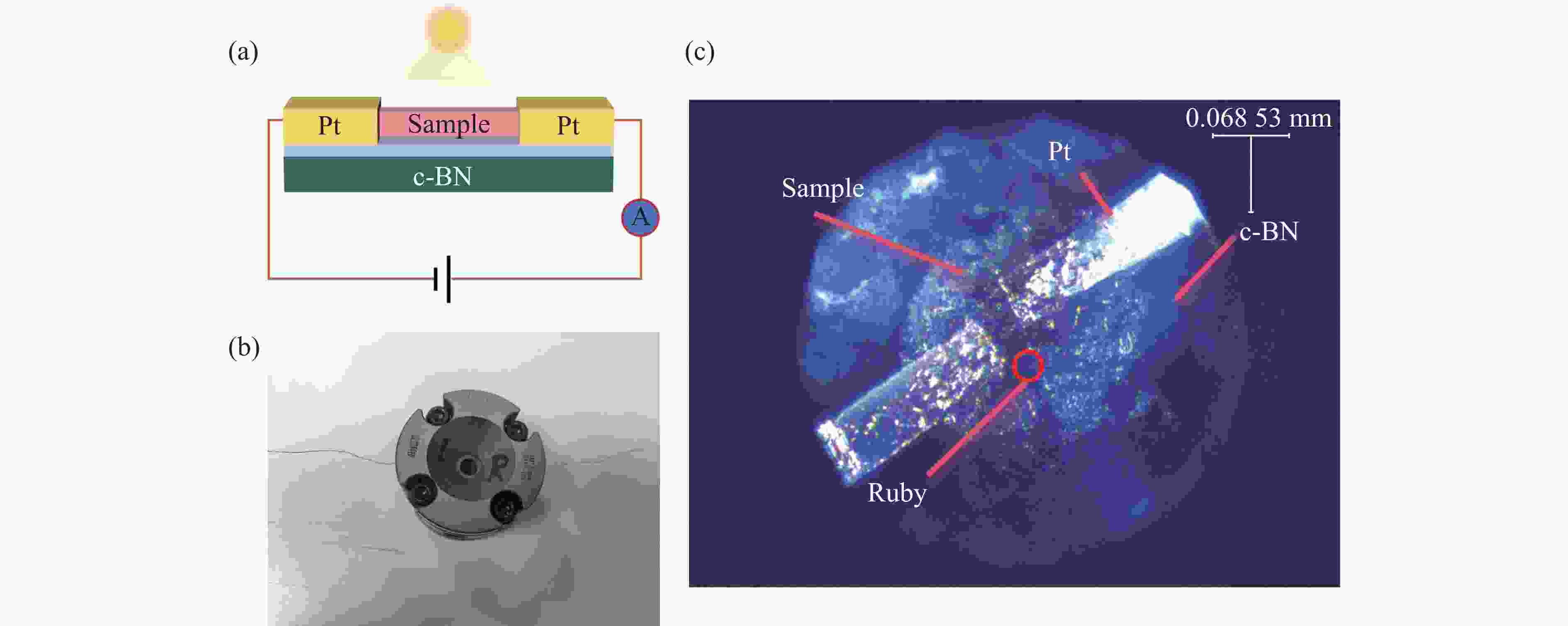
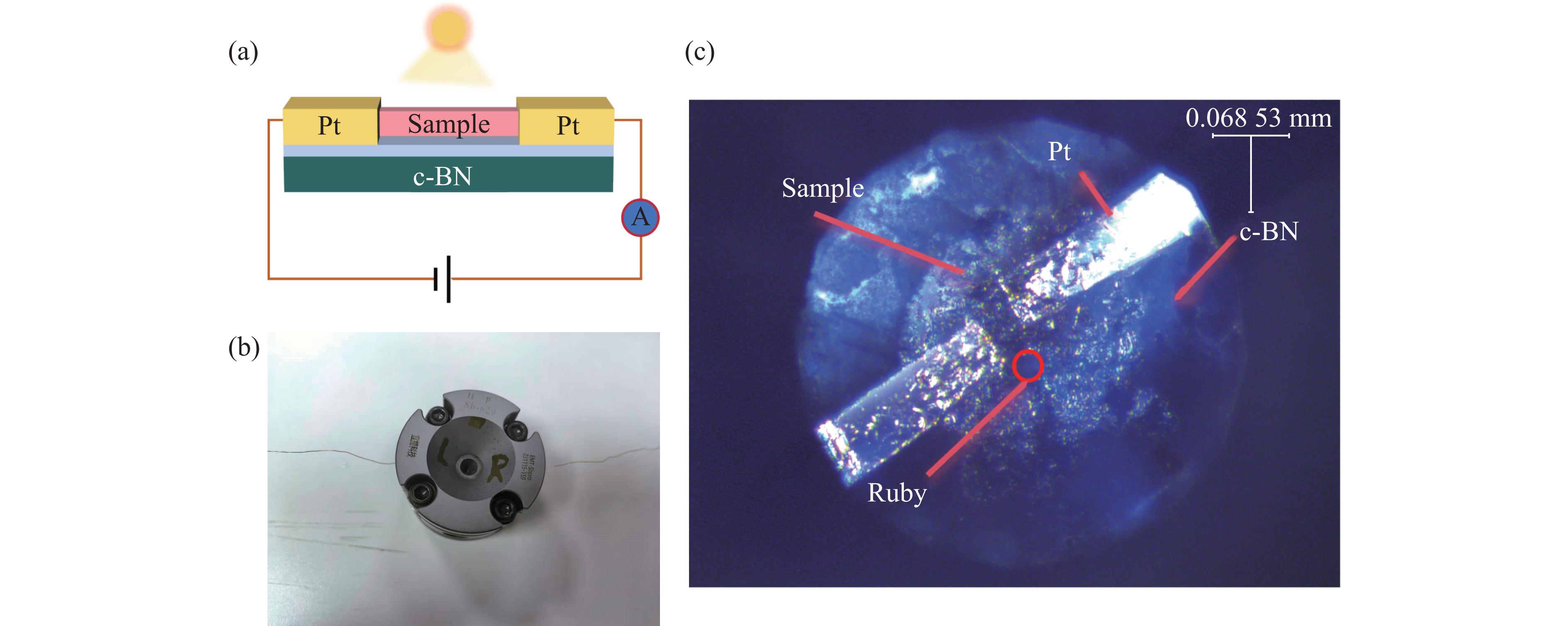
图 1 (a) 原位高压光电流测试原理图,(b) DAC装置外部实物照片,(c) 显微镜下样品腔内部结构俯视图
Figure 1. (a) Schematic diagram of the in-situ high-pressure photocurrent measurement; (b) photograph of the external DAC setup; (c) top-view optical microscope image showing the internal structure of the sample chamber
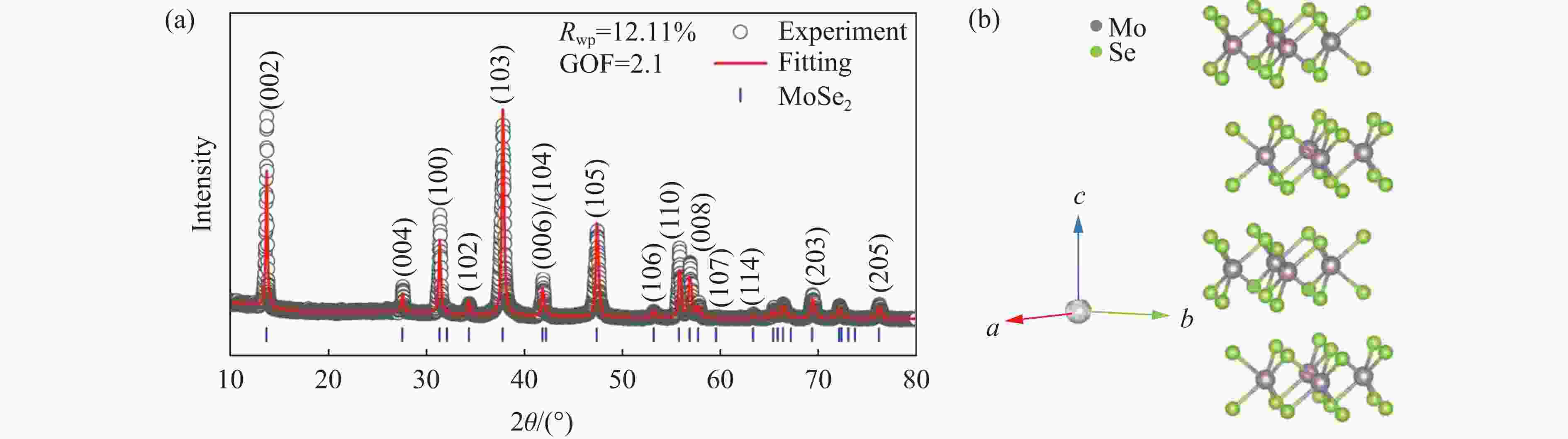
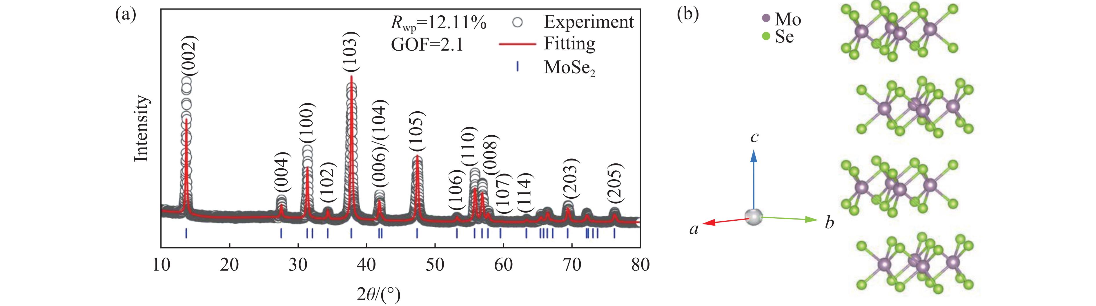
图 2 (a) MoSe2在常压下的XRD数据的Rietveld精修结果,(b) MoSe2的晶体结构示意图
Figure 2. (a) Rietveld refinement of XRD data of MoSe2 at ambient pressure; (b) schematic diagram of the crystal structure of MoSe2
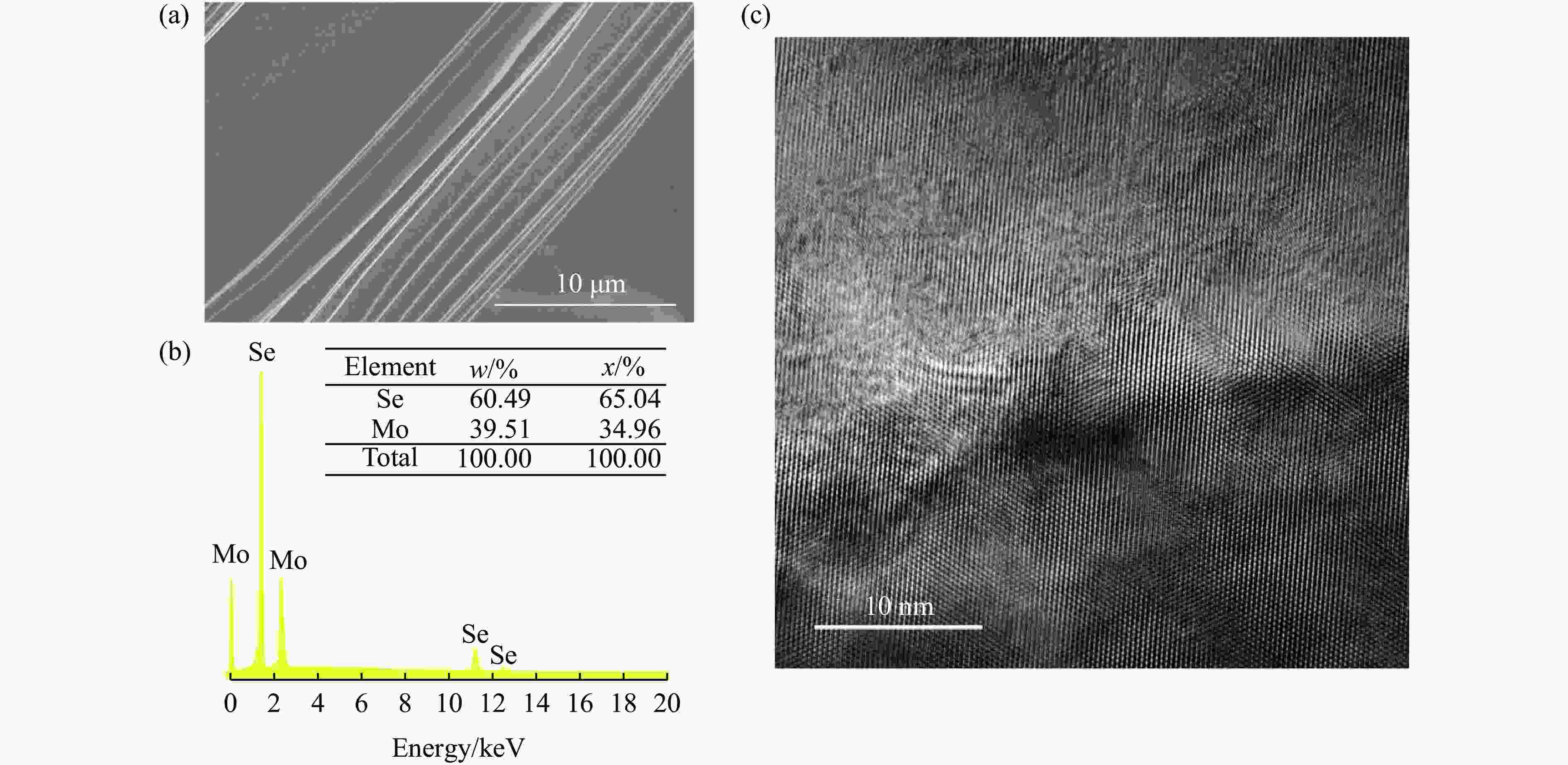
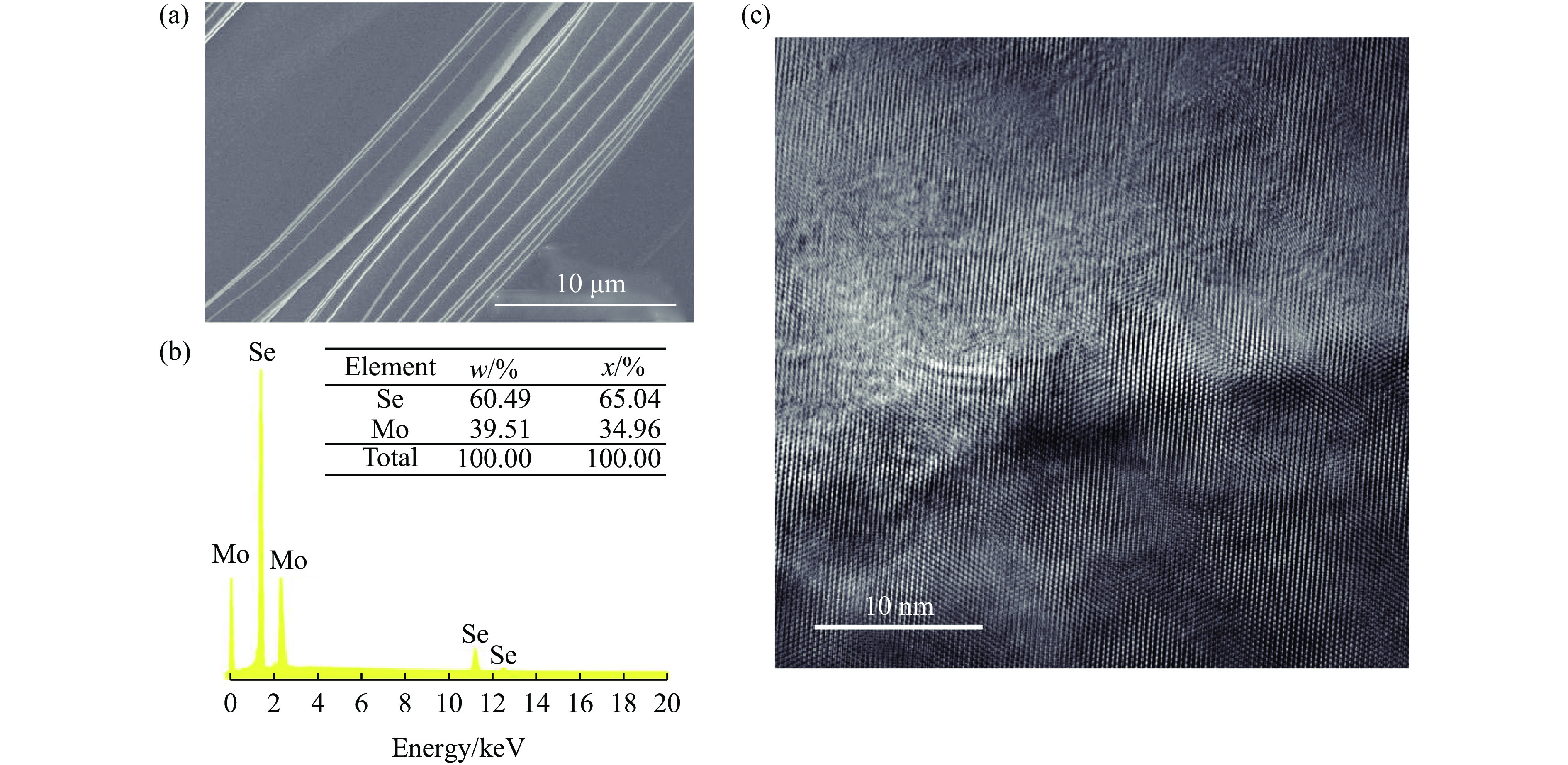
图 3 (a) MoSe2的SEM图像,(b) MoSe2的EDS能谱及元素组成,(c) MoSe2的TEM晶格图像
Figure 3. (a) SEM image of MoSe2; (b) EDS spectrum and elemental composition of MoSe2; (c) TEM lattice image of MoSe2
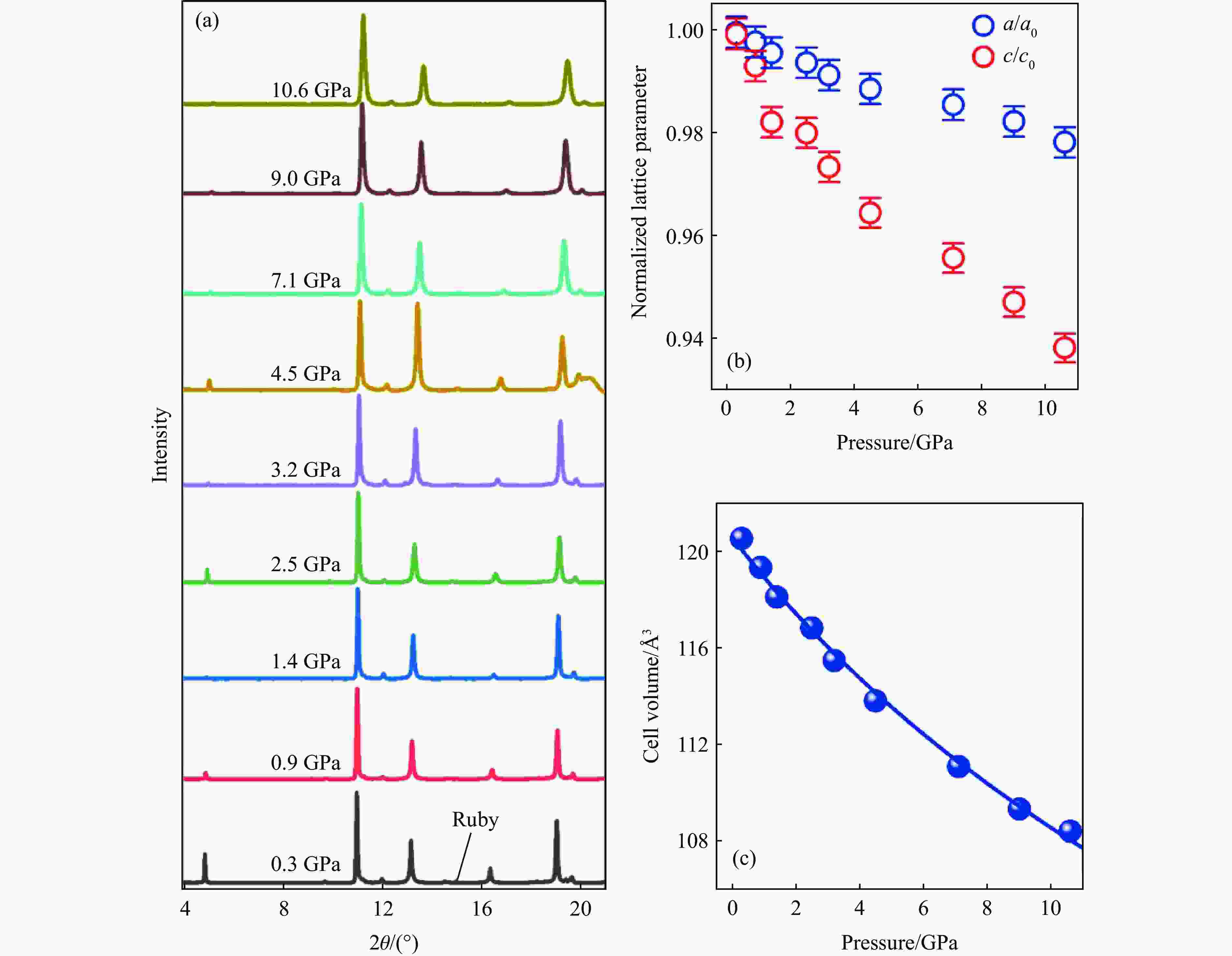
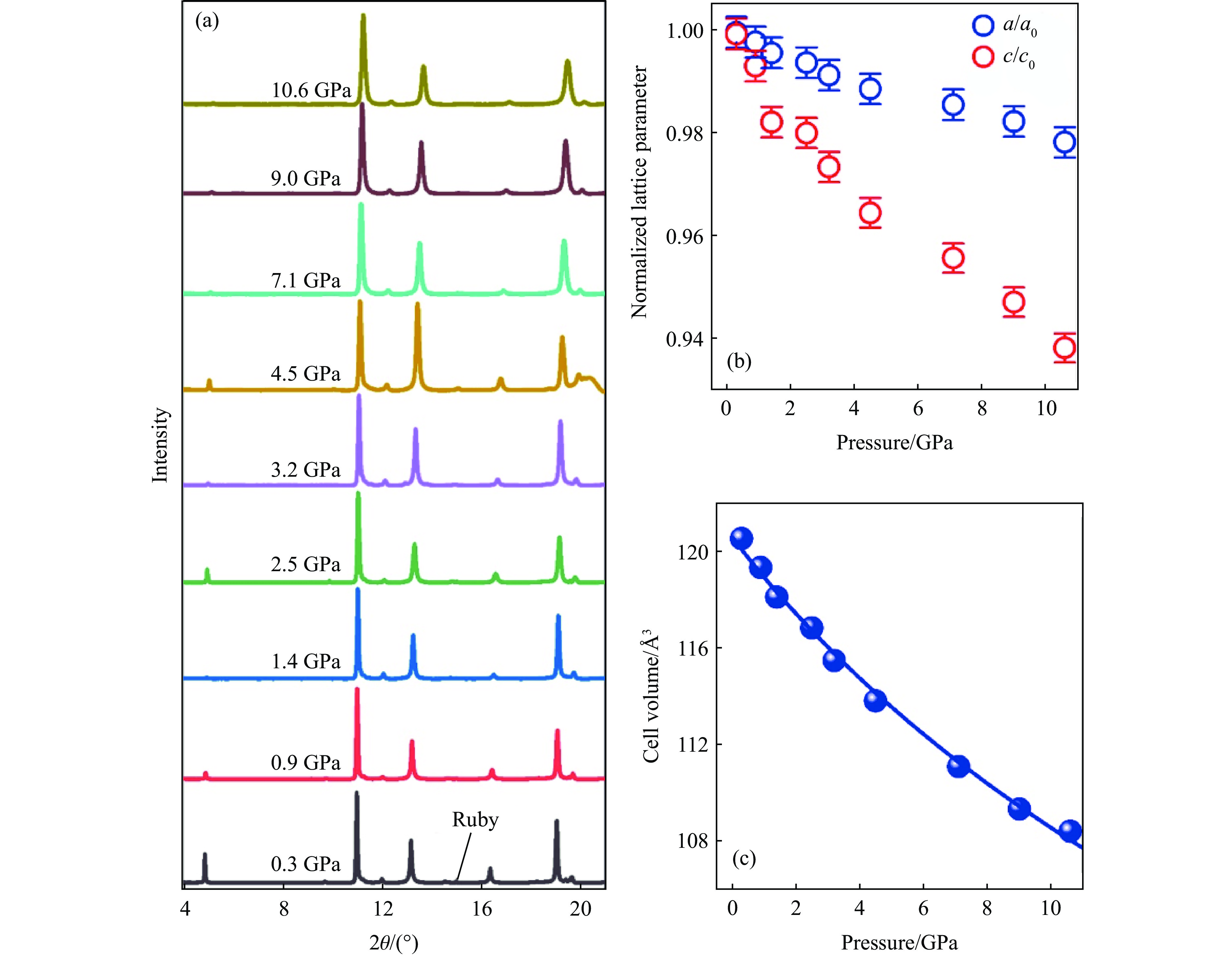
图 5 (a) 不同压力下MoSe2的原位XRD谱,(b) MoSe2的归一化晶格参数随压力的演化,(c) MoSe2的晶胞体积随压力的演化
Figure 5. (a) In-situ XRD patterns of MoSe2 at various pressures; (b) evolution of normalized lattice parameters of MoSe2 with pressure; (c) evolution of unit cell volume of MoSe2 with pressure
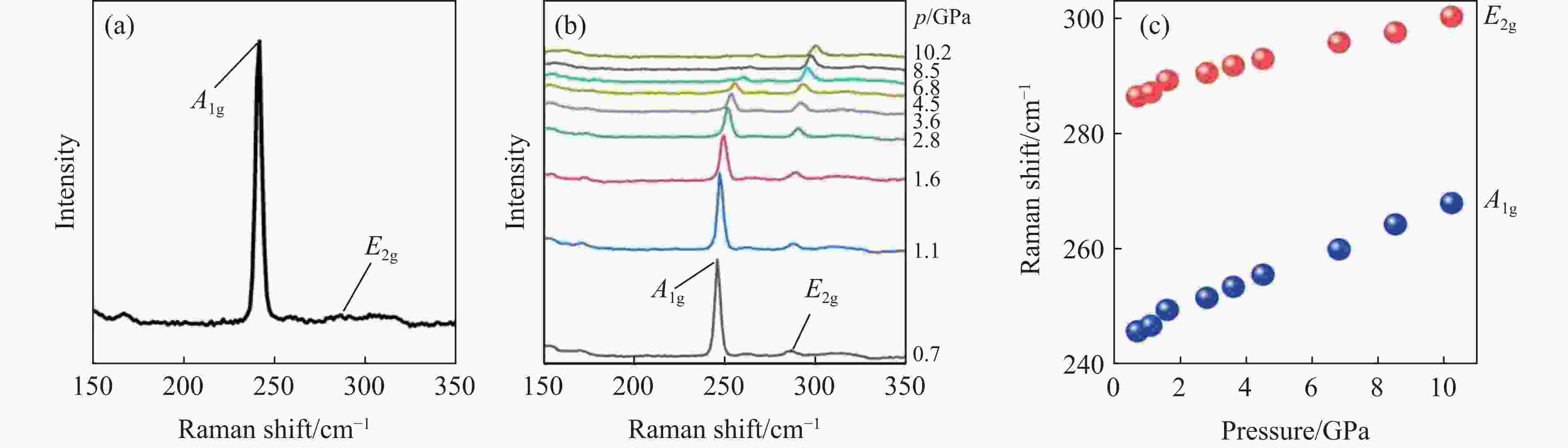
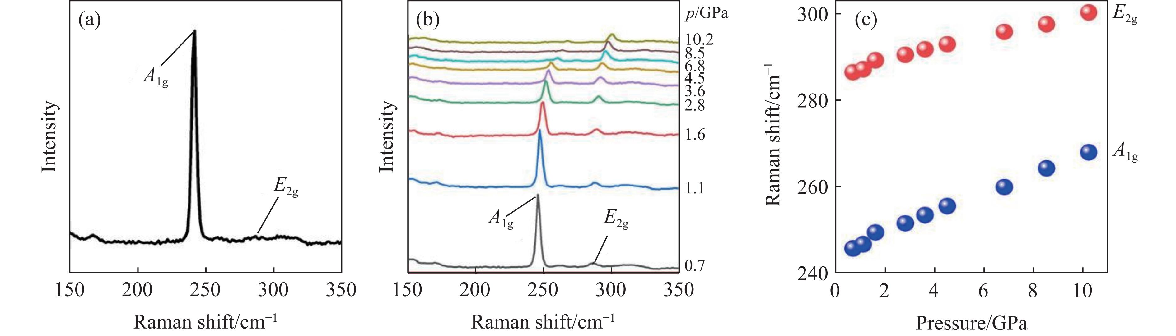
图 6 (a) 常压下MoSe2的原位拉曼光谱,(b) 不同压力下MoSe2的原位拉曼光谱,(c) E2g和A1g模式的拉曼频移随压力的演化
Figure 6. (a) Raman spectra of MoSe2 at ambient pressure; (b) in-situ Raman spectra of MoSe2 at various pressures; (c) evolution of Raman shifts of the E2g and A1g modes with pressure
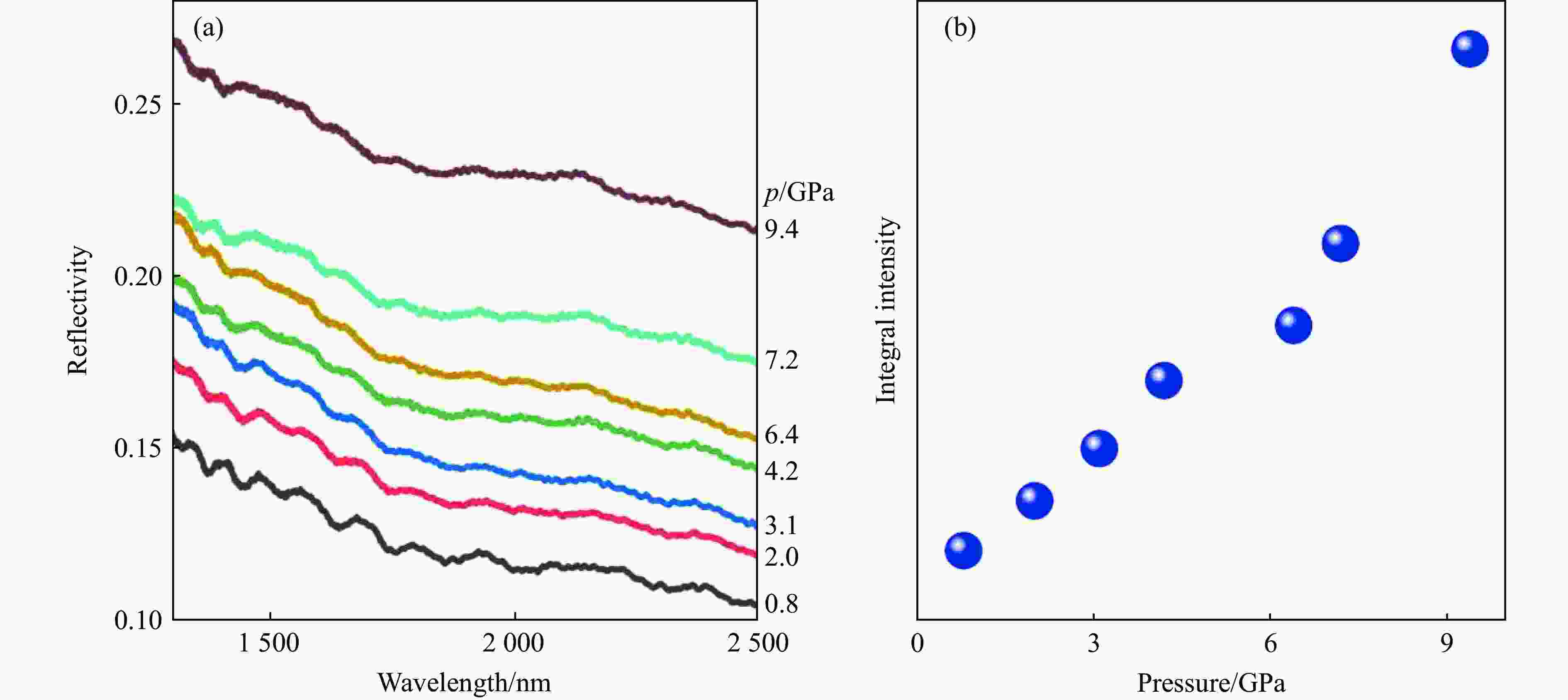
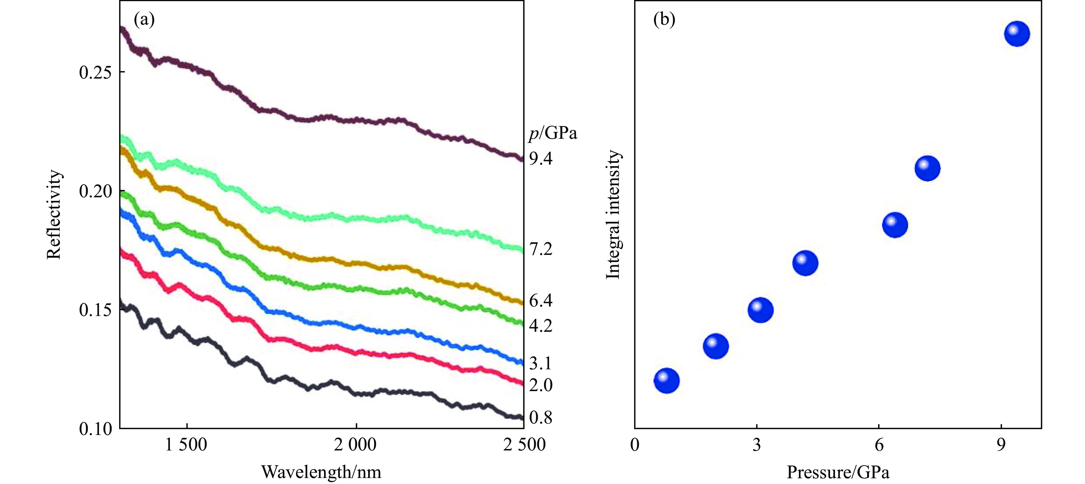
图 7 (a) 不同压力下MoSe2的近红外反射光谱,(b) 积分强度随压力的演化
Figure 7. (a) Near-infrared reflectivity spectra of MoSe2 at various pressures; (b) evolution of integral intensity with pressure
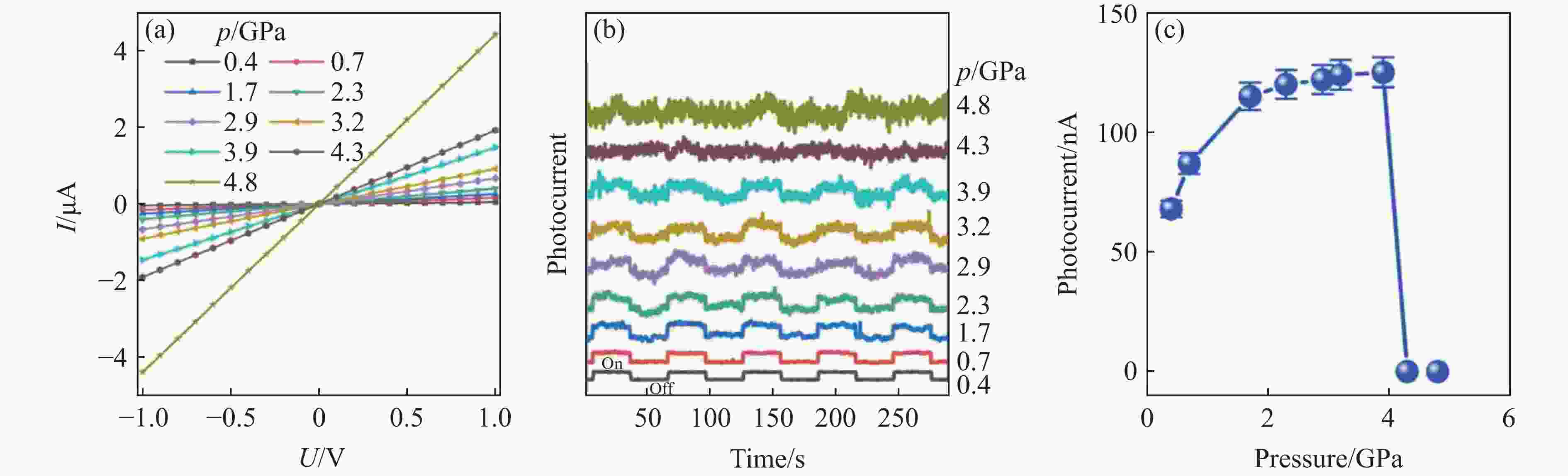
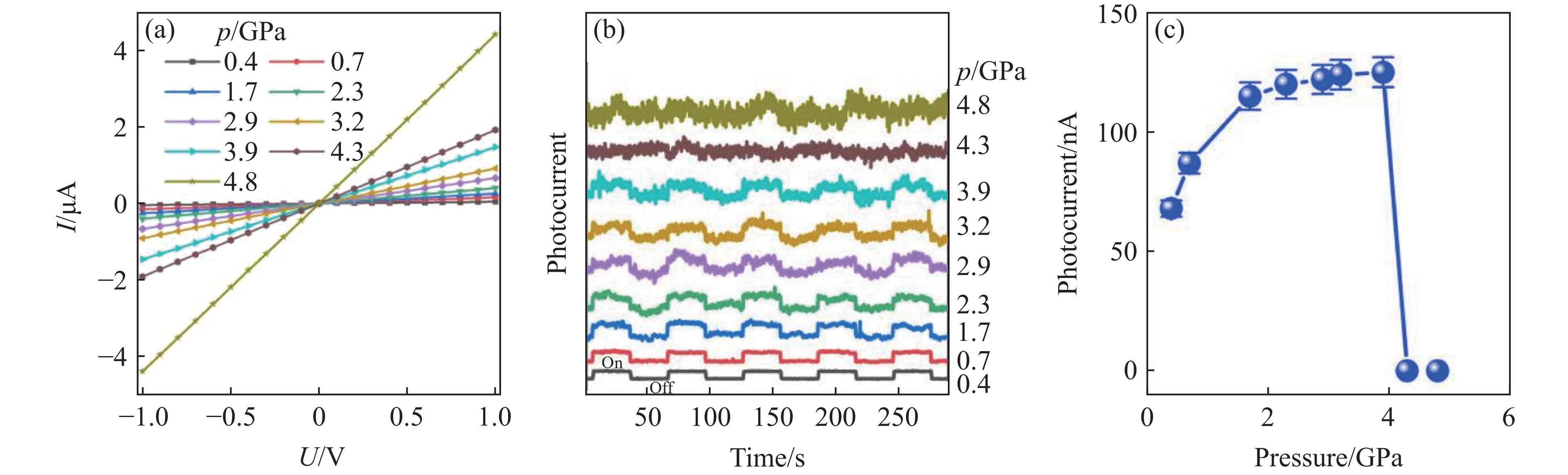
图 8 (a) MoSe2在不同压力下的I-U特性曲线,(b) 不同压力下光电流的时域响应(30 s光照/30 s暗态循环),(c) 光电流随压力的演化规律
Figure 8. (a) I-U characteristic curves of MoSe2 at various pressures; (b) time-dependent photocurrent response under periodic illumination (30 s light on/30 s light off cycles) at various pressures; (c) evolution of photocurrent as a function of pressure
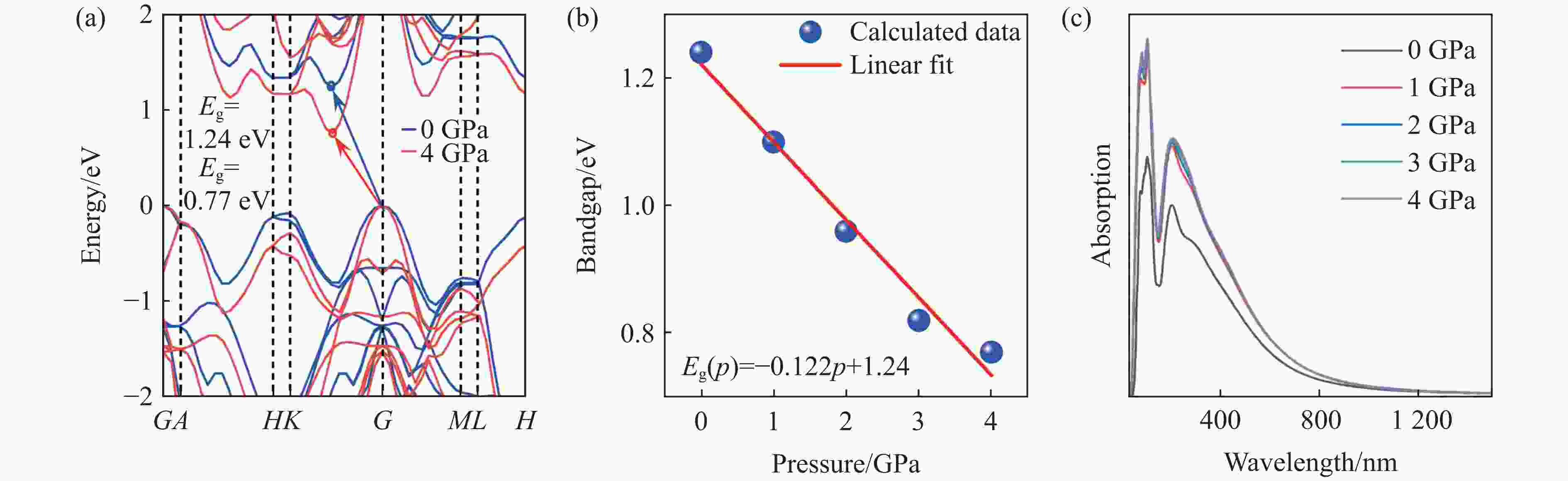
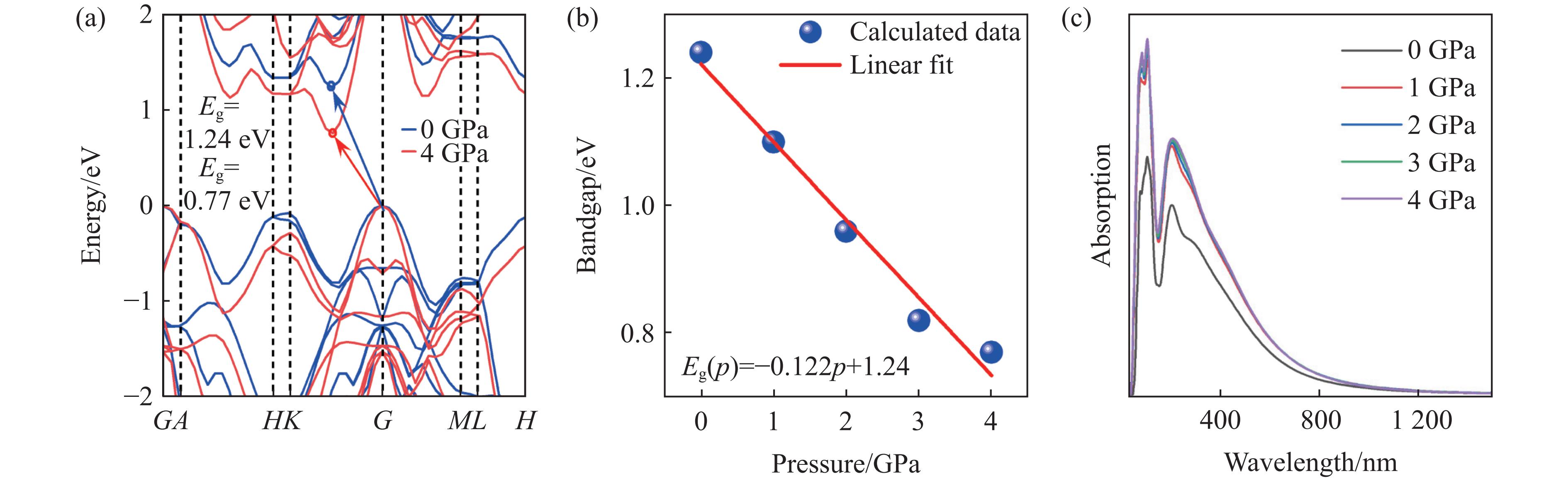
图 9 (a) MoSe2在不同压力下的能带结构,(b) 带隙随压力的线性演化关系,(c) 不同压力下的光吸收谱
Figure 9. (a) Calculated band structures of MoSe2 at different pressures; (b) linear evolution of bandgap as a function of pressure; (c) calculated optical absorption spectra at various pressures
表 1 高压下MoSe2的晶体结构参数
Table 1. Crystal structure parameters of MoSe2 under high pressure
p/GPa a/Å c/Å V/Å3 0 3.288 12.911 120.777 0.3 3.286 12.888 120.530 0.9 3.279 12.808 119.329 1.4 3.273 12.667 118.154 2.5 3.266 12.640 116.825 3.2 3.258 12.555 115.473 4.5 3.250 12.441 113.806 7.1 3.241 12.327 111.074 9.0 3.229 12.216 109.323 10.6 3.216 12.101 108.397  下载: 导出CSV
-
[1] ZOU X H, LIU X K, LI W Z, et al. Optoelectronic oscillators (OEOs) to sensing, measurement, and detection [J]. IEEE Journal of Quantum Electronics, 2016, 52(1): 0601116. doi: 10.1109/jqe.2015.2504088 [2] LAY-EKUAKILLE A, MASSARO A, SINGH S P, et al. Optoelectronic and nanosensors detection systems: a review [J]. IEEE Sensors Journal, 2021, 21(11): 12645–12653. doi: 10.1109/JSEN.2021.3055750 [3] JANG S, HWANG E, LEE Y, et al. Multifunctional graphene optoelectronic devices capable of detecting and storing photonic signals [J]. Nano Letters, 2015, 15(4): 2542–2547. doi: 10.1021/acs.nanolett.5b00105 [4] WOJTAS J, STACEWICZ T, BIELECKI Z, et al. Towards optoelectronic detection of explosives [J]. Opto-Electronics Review, 2013, 21(2): 210–219. doi: 10.2478/s11772-013-0082-x [5] ZHANG Y M, WANG Y C, WANG L F, et al. Highly sensitive photoelectric detection and imaging enhanced by the pyro-phototronic effect based on a photoinduced dynamic Schottky effect in 4H-SiC [J]. Advanced Materials, 2022, 34(35): 2204363. doi: 10.1002/adma.202204363 [6] WANG D, LI G Q. Advances in photoelectric detection units for imaging based on perovskite materials [J]. Laser & Photonics Reviews, 2022, 16(7): 2100713. doi: 10.1002/lpor.202100713 [7] LI Z H, JIN X, YUAN C F, et al. Photon detector technology for laser ranging: a review of recent developments [J]. Coatings, 2025, 15(7): 798. doi: 10.3390/coatings15070798 [8] JIANG B Q, HOU Y G, WU J X, et al. In-fiber photoelectric device based on graphene-coated tilted fiber grating [J]. Opto-Electronic Science, 2023, 2(6): 230012. doi: 10.29026/oes.2023.230012 [9] CHEN W L, ZHANG Z, LIU G. Retinomorphic optoelectronic devices for intelligent machine vision [J]. iScience, 2022, 25(1): 103729. doi: 10.1016/j.isci.2021.103729 [10] JANG H, LIU C Y, HINTON H, et al. An atomically thin optoelectronic machine vision processor [J]. Advanced Materials, 2020, 32(36): 2002431. doi: 10.1002/adma.202002431 [11] WU J, HAN L J, ZHANG Q C. Optoelectronic fiber devices: design, advancements, and perspectives [J]. Matter, 2026, 9(2): 102462. doi: 10.1016/j.matt.2025.102462 [12] YANO H, SASAKI G, MURATA M, et al. An ultra-high-speed optoelectronic integrated receiver for fiber-optic communications [J]. IEEE Transactions on Electron Devices, 1992, 39(10): 2254–2259. doi: 10.1109/16.158796 [13] METUH P, PETERSEN P M, OU Y Y. Recent advances in wireless optoelectronic biomedical implants [J]. Laser & Photonics Reviews, 2024, 18(12): 2300752. doi: 10.1002/lpor.202300752 [14] ZHANG H J, PENG Y X, ZHANG N H, et al. Emerging optoelectronic devices based on microscale LEDs and their use as implantable biomedical applications [J]. Micromachines, 2022, 13(7): 1069. doi: 10.3390/mi13071069 [15] CHEN X L, LU X B, DENG B C, et al. Widely tunable black phosphorus mid-infrared photodetector [J]. Nature Communications, 2017, 8(1): 1672. doi: 10.1038/s41467-017-01978-3 [16] LI Y Z, HE X, CHEN S C, et al. Intelligent photodetectors: postmanufacturing tunability toward enhanced performance and advanced functions [J]. Chemical Reviews, 2025, 125(15): 6977–7022. doi: 10.1021/acs.chemrev.4c00763 [17] WANG W B, ZHANG F J, LI L L, et al. Highly sensitive polymer photodetectors with a broad spectral response range from UV light to the near infrared region [J]. Journal of Materials Chemistry C, 2015, 3(28): 7386–7393. doi: 10.1039/C5TC01383F [18] KONSTANTATOS G, CLIFFORD J, LEVINA L, et al. Sensitive solution-processed visible-wavelength photodetectors [J]. Nature Photonics, 2007, 1(9): 531–534. doi: 10.1038/nphoton.2007.147 [19] REZAEI M, BIANCONI S, LAUHON L J, et al. A new approach to designing high-sensitivity low-dimensional photodetectors [J]. Nano Letters, 2021, 21(23): 9838–9844. doi: 10.1021/acs.nanolett.1c03665 [20] WANG J, JIAO H X, WANG X D, et al. High-sensitivity GaN UV photodetector integrated with graphene [J]. Applied Physics Letters, 2025, 126(17): 173503. doi: 10.1063/5.0260828 [21] LI J B, MA W L, JIANG L, et al. High performance of room-temperature NbSe2 terahertz photoelectric detector [J]. ACS Applied Materials & Interfaces, 2022, 14(12): 14331–14341. doi: 10.1021/acsami.2c00175 [22] LU Y P. Short distance detection and control system based on photoelectric sensor and its application in target detection of handling robot [J]. Journal of Nanoelectronics and Optoelectronics, 2023, 18(8): 964–970. doi: 10.1166/jno.2023.3467 [23] QIN W Q, MA T J, FAN X H, et al. Optical sensing technologies for gas-insulated equipment: advances and perspectives [J]. CSEE Journal of Power and Energy Systems, 2025, 11(6): 2983–3011. doi: 10.17775/cseejpes.2025.05930 [24] YILDIRIM K, NAGARAJAN B, TJAHJOWIDODO T, et al. Development of a multi-sensor system for in-situ process monitoring of femtosecond laser micromachining [J]. The International Journal of Advanced Manufacturing Technology, 2024, 135(1/2): 799–813. doi: 10.1007/s00170-024-14580-x [25] CHAN V W S, HALL K L, MODIANO E, et al. Architectures and technologies for high-speed optical data networks [J]. Journal of Lightwave Technology, 1998, 16(12): 2146–2168. doi: 10.1109/50.736582 [26] CHE D, DEAKIN C, CHEN X, et al. 440-GBaud all-electronic signaling enabling single-wavelength net rate over 1 Tb/s per modulation dimension [J]. Journal of Lightwave Technology, 2026, 44(3): 1178–1193. doi: 10.1109/JLT.2025.3632244 [27] POLAT E O, MERCIER G, NIKITSKIY I, et al. Flexible graphene photodetectors for wearable fitness monitoring [J]. Science Advances, 2019, 5(9): eaaw7846. doi: 10.1126/sciadv.aaw7846 [28] EBRAHIMI Z, GOSSELIN B. Photodetector innovations for advancing wearable optical biosensors: a review [J]. IEEE Sensors Journal, 2025, 25(3): 4070–4095. doi: 10.1109/jsen.2024.3515893 [29] SCLAR N. Properties of doped silicon and Germanium infrared detectors [J]. Progress in Quantum Electronics, 1984, 9(3): 149–257. doi: 10.1016/0079-6727(84)90001-6 [30] WANG K L, CHA D, LIU J L, et al. Ge/Si self-assembled quantum dots and their optoelectronic device applications [J]. Proceedings of the IEEE, 2007, 95(9): 1866–1883. doi: 10.1109/JPROC.2007.900971 [31] WANG H Y, LI Z X, LI D Y, et al. Van der Waals integration based on two-dimensional materials for high-performance infrared photodetectors [J]. Advanced Functional Materials, 2021, 31(30): 2103106. doi: 10.1002/adfm.202103106 [32] WANG J L, FANG H H, WANG X D, et al. Recent progress on localized field enhanced two-dimensional material photodetectors from ultraviolet-visible to infrared [J]. Small, 2017, 13(35): 1700894. doi: 10.1002/smll.201700894 [33] HEINE T. Transition metal chalcogenides: ultrathin inorganic materials with tunable electronic properties [J]. Accounts of Chemical Research, 2015, 48(1): 65–72. doi: 10.1021/ar500277z [34] JOHARI P, SHENOY V B. Tuning the electronic properties of semiconducting transition metal dichalcogenides by applying mechanical strains [J]. ACS Nano, 2012, 6(6): 5449–5456. doi: 10.1021/nn301320r [35] PAN L F, ZOU B S, SHI L J. Electric field modulation of the band gap, dielectric constant and polarizability in SnS atomically thin layers [J]. Physics Letters A, 2016, 380(27/28): 2227–2232. doi: 10.1016/j.physleta.2016.04.044 [36] HEMLEY R J. Effects of high pressure on molecules [J]. Annual Review of Physical Chemistry, 2000, 51: 763–800. doi: 10.1146/annurev.physchem.51.1.763 [37] HAZEN R M, FINGER L W. Bulk moduli and high-pressure crystal structures of rutile-type compounds [J]. Journal of Physics and Chemistry of Solids, 1981, 42(3): 143–151. doi: 10.1016/0022-3697(81)90074-3 [38] ZHANG L J, WANG Y C, LV J, et al. Materials discovery at high pressures [J]. Nature Reviews Materials, 2017, 2(4): 17005. doi: 10.1038/natrevmats.2017.5 [39] FU L, WAN Y, TANG N, et al. K-Λ crossover transition in the conduction band of monolayer MoS2 under hydrostatic pressure [J]. Science Advances, 2017, 3(11): e1700162. doi: 10.1126/sciadv.1700162 [40] ZHANG X T, DONG Q, LI Z L, et al. Significant pressure-induced enhancement of photoelectric properties of WS2 in the near-infrared region [J]. Materials Research Letters, 2022, 10(8): 547–555. doi: 10.1080/21663831.2022.2065893 [41] LI Z L, LI Q J, LI H Y, et al. Pressure-tailored band engineering for significant enhancements in the photoelectric performance of CsI3 in the optical communication waveband [J]. Advanced Functional Materials, 2022, 32(8): 2108636. doi: 10.1002/adfm.202108636 [42] SHUAI J, MAO J, SONG S W, et al. Tuning the carrier scattering mechanism to effectively improve the thermoelectric properties [J]. Energy & Environmental Science, 2017, 10(3): 799–807. doi: 10.1039/C7EE00098G [43] ZHANG N, JALIL A, WU D X, et al. Refining defect states in W18O49 by Mo doping: a strategy for tuning N2 activation towards solar-driven nitrogen fixation [J]. Journal of the American Chemical Society, 2018, 140(30): 9434–9443. doi: 10.1021/jacs.8b02076 [44] BOUANGEUNE D, SHIM K H, LEEM S J, et al. Investigation of the surge immunity of monocrystalline silicon photovoltaic modules using dark current-voltage and 1/f noise power spectrum density characteristics [J]. Journal of Computational and Theoretical Nanoscience, 2015, 12(5): 751–755. doi: 10.1166/jctn.2015.3797 [45] SAI H Y, WANG L J, ZHANG J, et al. Portable device to assist with force control in ultrasound acquisition [J]. IEEE Transactions on Ultrasonics, Ferroelectrics, and Frequency Control, 2023, 70(9): 930–943. doi: 10.1109/tuffc.2022.3181287 [46] GUSAKOVA J, WANG X L, SHIAU L L, et al. Electronic properties of bulk and monolayer TMDs: theoretical study within DFT framework (GVJ-2e method) [J]. Physica Status Solidi (A), 2017, 214(12): 1700218. doi: 10.1002/pssa.201700218 [47] MAO H K, BELL P M, SHANER J W, et al. Specific volume measurements of Cu, Mo, Pd, and Ag and calibration of the ruby R1 fluorescence pressure gauge from 0.06 to 1 Mbar [J]. Journal of Applied Physics, 1978, 49(6): 3276–3283. doi: 10.1063/1.325277 [48] BARTOLOTTI L J, FLURCHICK K. An introduction to density functional theory [M]//LIPKOWITZ K B, BOYD D B. Reviews in Computational Chemistry. New York: Wiley-VCH, 1996: 187–216. [49] ERNZERHOF M, SCUSERIA G E. Assessment of the Perdew-Burke-Ernzerhof exchange-correlation functional [J]. The Journal of Chemical Physics, 1999, 110(11): 5029–5036. doi: 10.1063/1.478401 [50] ZHAO Z, ZHANG H J, YUAN H T, et al. Pressure induced metallization with absence of structural transition in layered molybdenum diselenide [J]. Nature Communications, 2015, 6: 7312. doi: 10.1038/ncomms8312 [51] NAM D, LEE J U, CHEONG H. Excitation energy dependent Raman spectrum of MoSe2 [J]. Scientific Reports, 2015, 5: 17113. doi: 10.1038/srep17113 [52] LI Z Y, WANG Y M, ZENG X H, et al. Pressure-regulated bandgap narrowing and photoelectric activity enhancement in layered halide compound GeI2 [J]. Journal of Applied Physics, 2025, 137(8): 085902. doi: 10.1063/5.0256512 -

 下载:
下载:

计量
- 文章访问数: 660
- HTML全文浏览量: 256
- PDF下载量: 58
